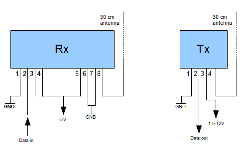
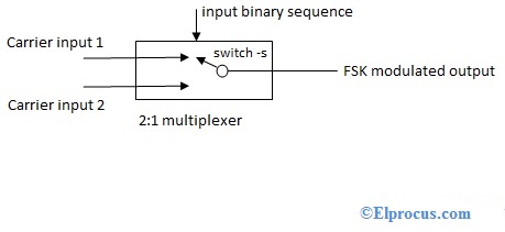
25+ fsk transmitter and receiver circuit diagram
Ultrasonic transmitter circuit The transmitter circuit Fig1 is built around two CD4017 decade counter ICs IC1 and IC2 D-type flip-flop IC CD4013 IC3 and a few discrete. Set up a QFSK link with a data rate of 2Kbps and a frequency separation of 8KHz a.
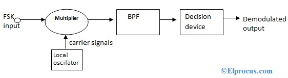
Frequency Shift Keying Fsk Working Advantages And Disadvantages
File under Integrated Circuits IC01 1999 Jan 22 INTEGRATED CIRCUITS UAA3220TS Frequency Shift Keying.
. Low Pass Filter Design The other thing that must be done in converting the block. NAVALPOSTGRADUATESCHOOL MontereyCalifornia THESIS 2FSKQPSKTRANSMITTERANDRECEIVER. Verify the spectrum at the receiver is as expected.
The ADF7020-1 is a low power highly integrated FSKGFSK ASKOOKGOOK transceiver designed for operation in the low UHF and VHF bands. Here the circuit diagram of laser receiver. The purpose of this page is to make the circuit diagrams available for educational purposes.
Shown in Fig9 the UAA3220TS works as an FSK receiver. Here is a simple infrared detector circuit which gives a LED indication. FSK system demodulator system simulated as a discrete-time system at a sampling rate of fsamp.
Sound signals in this circuit travel by shifting the carrier wave frequencies. I wont be able to help you contructing them or give more info than what is written on this page. An FM Frequency modulation circuit represents wireless communication enabled by a BJT or a single transistor.
So we are using a PNP transistor. That it is synchronized with the transmitter. When IR rays fall on the TSOP then by the.
The audio signal transmitted by the laser diode LD1 is received by the calculators solar panel and amplified by IC2. In this section of circuit we are using a single transistor BD 139 which is a medium power transistorThe figure is shown above on left side of the pictureThe Bd139. The gain of the amplifier is fixed.
It can be calculated using this. Conceptually and in fact the transmitter could consist of two oscillators on frequencies f1 and f2 with only one being connected to the output at any one time. As you can see in the blow IR Transmitter Circuit We have used 1k R1 20K R2 and 1nF capacitor to generate the frequency of approx.
The ADF7020-1 uses an external VCO inductor. Automatic gain control circuit has used to provide efficient frequency offset estimation and control the system gain as possible. The optimized HDL completion flow chart is planned.
TSOP gives active low output. This is shown in block.
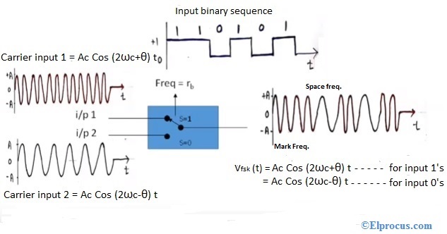
Frequency Shift Keying Fsk Working Advantages And Disadvantages
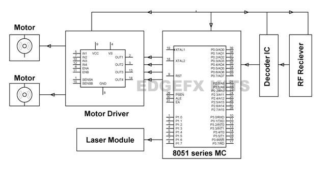
Rf Communication Protocols And Its Applications
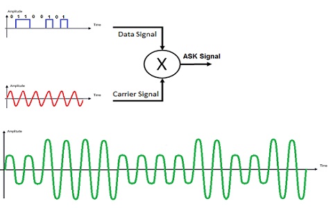
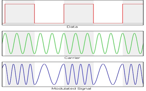
Amplitude Shift Keying Circuit Diagram Working And Its Applications
Frequency Shift Keying Fsk Working Advantages And Disadvantages
Rf Communication Protocal For Industrial And Home Applications
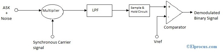
Amplitude Shift Keying Circuit Diagram Working And Its Applications
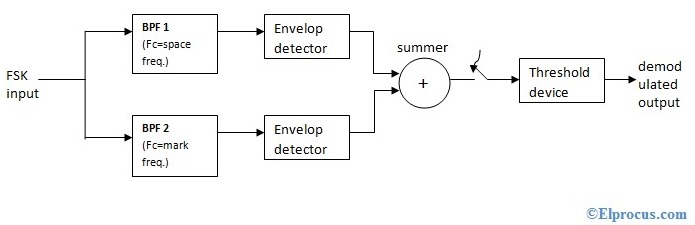
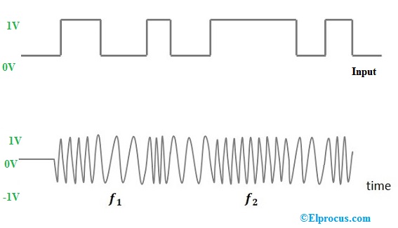
Frequency Shift Keying Fsk Working Advantages And Disadvantages
Digital Modulation Types And Differences Between Analog And Digital
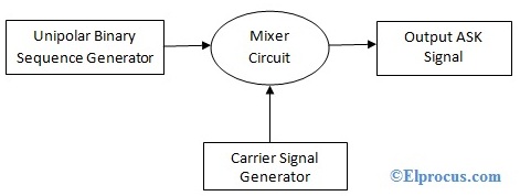
Amplitude Shift Keying Circuit Diagram Working And Its Applications
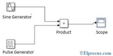
Amplitude Shift Keying Circuit Diagram Working And Its Applications
Frequency Shift Keying Fsk Working Advantages And Disadvantages
2
![]()
Power Line Carrier Communication Circuit Diagram And Its Working
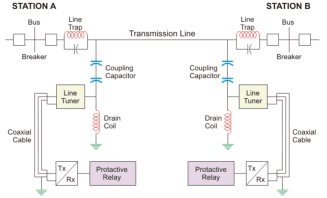
Power Line Carrier Communication Circuit Diagram And Its Working
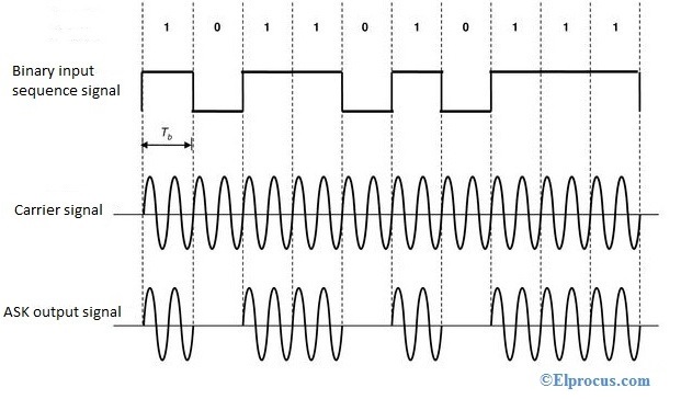
Amplitude Shift Keying Circuit Diagram Working And Its Applications
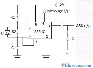
Amplitude Shift Keying Circuit Diagram Working And Its Applications
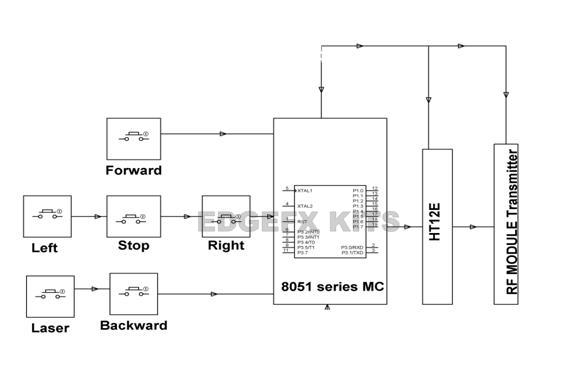
Rf Communication Protocal For Industrial And Home Applications